- Company Articles
- Products and Technology
- Application Cases
- Aluminum Honeycomb Panels in Semiconductor Manufacturing: Contamination Control Benefits

Aluminum Honeycomb Panels in Semiconductor Manufacturing: Contamination Control Benefits
Related Product
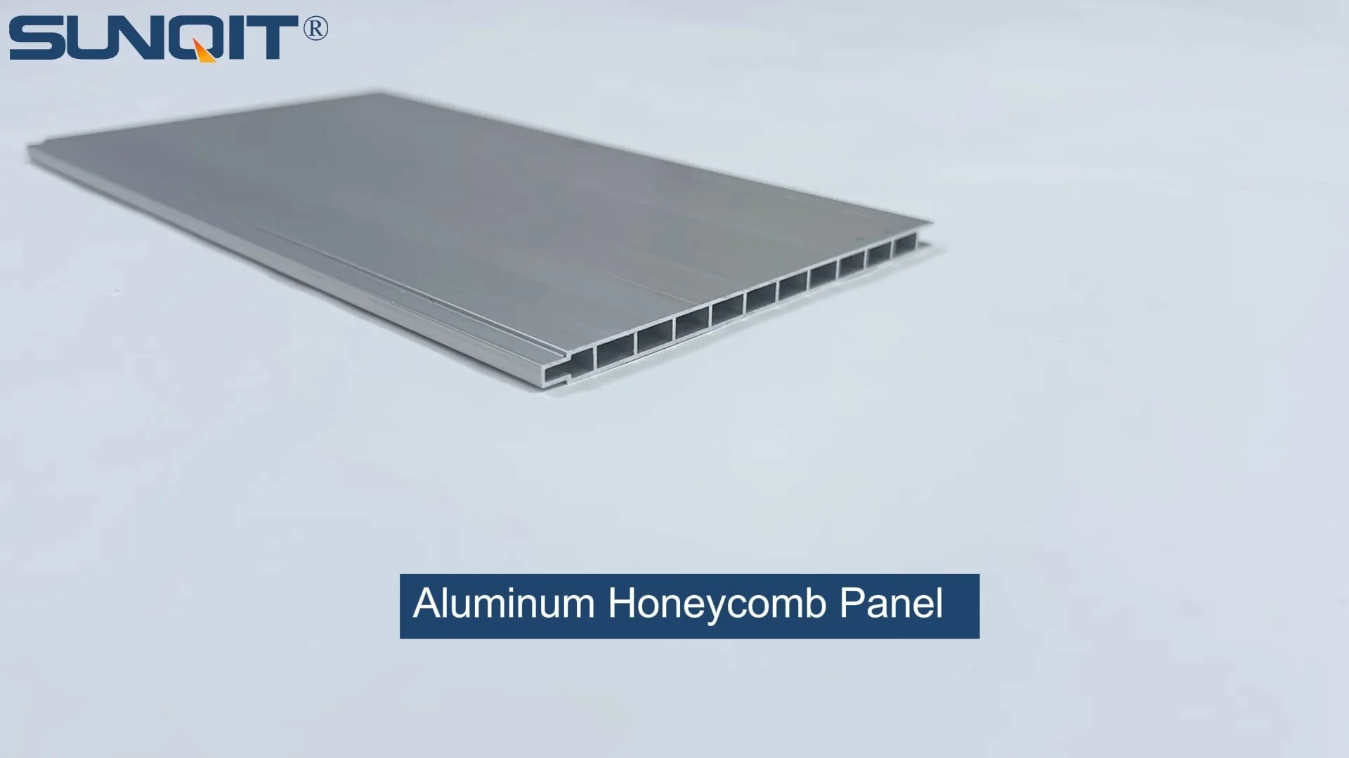
Aluminum Honeycomb Panel
Aluminum honeycomb panel used as table top, side wall, it is connected one pcs by one pcs from the side slot to make a full pieces.This panel width 105mm, 55mm, 35mm are optional for slection.
In the high-stakes world of semiconductor manufacturing, where the difference between a functional chip and a costly failure can be measured in nanometers, the battle against contamination is never-ending. Imagine a single dust particle—smaller than the width of a human hair—landing on a 3nm transistor. That tiny speck could disrupt electron flow, render the chip useless, and erase thousands of dollars in production costs in an instant. For fab managers and process engineers, creating an environment that minimizes such risks isn't just a priority; it's the foundation of reliable, high-yield manufacturing. Among the array of tools and technologies designed to protect semiconductor wafers, one material has quietly emerged as a game-changer: the aluminum honeycomb panel. More than just a lightweight alternative to traditional materials, these panels are redefining how cleanrooms, workstations, and material handling systems approach contamination control. In this article, we'll explore why aluminum honeycomb panels are becoming indispensable in semiconductor fabs, how they integrate with critical systems like ESD workstations and lean manufacturing setups, and why their unique properties make them a superior choice for the industry's most demanding environments.
The Invisible Enemy: Contamination in Semiconductor Fabrics
To understand the value of aluminum honeycomb panels, we first need to grasp the magnitude of the contamination challenge in semiconductor manufacturing. Contamination comes in many forms, each with the potential to derail production. Particulate contamination—tiny solid or liquid particles suspended in air or deposited on surfaces—is the most visible threat. These particles can originate from anything: the air handling system, equipment lubricants, even the clothing of personnel. A 0.1-micron particle (about 1/500th the diameter of a human hair) is large enough to block a 3nm transistor, while chemical contaminants like residues from cleaning agents or outgassing from plastics can corrode delicate circuit patterns. Then there's electrostatic discharge (ESD), an invisible force that can damage chips without any visible sign of harm, turning functional wafers into scrap during handling or assembly.
The impact of contamination is staggering. Industry studies estimate that particulate contamination alone accounts for 20-30% of yield losses in advanced semiconductor fabrication. For a fab producing 5nm chips, where a single wafer can contain over 100,000 dies, even a 1% yield reduction translates to millions in lost revenue annually. Worse, contamination-related defects often aren't detected until late in the production process, after layers of lithography, etching, and deposition have already been applied—amplifying the cost of failure.
Traditional solutions to contamination control have focused on cleanroom design (HEPA filters, laminar airflow), strict gowning protocols, and specialized cleaning agents. But these measures only address the external environment. The materials used in the fab itself—workstation surfaces, material racks, conveyor systems—can be silent sources of contamination. For example, solid aluminum workbenches, while rigid, are heavy and prone to vibrating during use, dislodging particles from their surfaces. Plywood or composite panels, often used for cost savings, are porous, trapping dust and releasing volatile organic compounds (VOCs) that contaminate the air. Even stainless steel, though durable, can generate metallic particles through friction or corrosion, especially in high-humidity cleanrooms. The industry needed a material that could address these flaws—one that was lightweight, rigid, easy to clean, and resistant to particle generation and ESD. Enter aluminum honeycomb panels.
Aluminum Honeycomb Panels: Engineering for Cleanliness
At first glance, an aluminum honeycomb panel might look like any other flat sheet, but its magic lies in its structure. Imagine a sandwich where the "bread" is two thin sheets of aluminum (the skins) and the "filling" is a hexagonal honeycomb core made from ultra-thin aluminum foil, bonded together with high-strength adhesive. This design isn't arbitrary—it's the result of decades of materials science, optimized to deliver exceptional performance in weight-sensitive, high-precision applications.
The honeycomb core is the star of the show. By arranging aluminum foil into a repeating hexagonal pattern, engineers create a structure that's both incredibly lightweight and surprisingly rigid. A typical aluminum honeycomb panel with 1mm-thick skins and a 20mm core weighs just 4-6 kg per square meter—less than half the weight of a solid aluminum sheet of the same thickness. Yet, its bending rigidity (a measure of resistance to warping) is comparable to solid aluminum, thanks to the core's ability to distribute stress evenly across the panel. This combination of lightness and strength is critical in semiconductor fabs, where heavy equipment and workstations can strain floor load limits and vibrate excessively, generating particles. A lighter workstation is easier to move, reduces wear on casters and flooring, and minimizes vibration-related particle shedding.
But it's the panel's surface properties that truly set it apart for contamination control. Unlike porous materials like wood or some composites, the aluminum skins are non-porous and smooth, leaving no crevices for dust, moisture, or bacteria to hide. When properly finished—often with an anodized coating or a specialized ESD-resistant layer—the surface becomes easy to clean with standard cleanroom solvents, reducing the risk of chemical residue buildup. What's more, the aluminum itself is inherently inert, meaning it doesn't outgas VOCs or release particles even under the thermal cycling common in semiconductor processes (e.g., rapid temperature changes during wafer baking or deposition). For fabs operating under ISO 14644-1 Class 5 or stricter cleanroom standards (allowing fewer than 352 particles of 0.1 microns per cubic meter), this low outgassing profile is non-negotiable.

Contamination Control Benefits: Beyond the Surface
The advantages of aluminum honeycomb panels for contamination control go far beyond their smooth, non-porous surfaces. Let's break down how they address specific contamination risks in semiconductor manufacturing:
1. Minimizing Particle Generation
In a cleanroom, every material is a potential particle source. When equipment vibrates, when workers lean on workbenches, or when tools are placed and removed from surfaces, microscopic particles can flake off, becoming airborne and threatening wafers. Aluminum honeycomb panels mitigate this in two ways. First, their lightweight, rigid structure reduces vibration: when a technician places a tool on a honeycomb-panel workstation, the panel absorbs impact energy more effectively than a solid aluminum or wood surface, minimizing the shaking that dislodges particles. Second, the aluminum skins are highly resistant to abrasion and wear. Unlike painted steel or plastic, which can chip or scratch over time, anodized aluminum skins maintain their integrity even after repeated cleaning and contact with tools, reducing the risk of particle shedding from surface degradation.
2. ESD Protection: Safeguarding Sensitive Electronics
Electrostatic discharge is a silent killer in semiconductor manufacturing. A static charge of just 100 volts can damage a 3nm chip, and charges can build up on work surfaces, tools, or even personnel without warning. Aluminum honeycomb panels, when treated with a conductive coating (often a clear, anodized layer doped with conductive particles), act as effective ESD shields. The conductive skins provide a low-resistance path to ground, ensuring that any static charge generated during wafer handling or tool use is safely dissipated before it can reach the chips. This makes them ideal for integration into ESD workstations—the specialized benches where wafers are inspected, assembled, or tested. Unlike non-conductive materials like plastic or wood, which can insulate and hold static charges, aluminum honeycomb panels actively prevent charge buildup, turning the workstation itself into a protective barrier.
3. Thermal Stability: Reducing Contamination from Warping
Semiconductor processes are thermally intensive. Wafers are heated to hundreds of degrees during deposition, cooled rapidly during etching, and exposed to temperature gradients that can cause materials to expand or contract. For work surfaces and material racks, thermal stability is critical—warping or bowing under heat can create gaps where particles accumulate or misalign wafers during transport. Aluminum honeycomb panels excel here: the aluminum skins and core have the same thermal expansion coefficient, ensuring the panel expands and contracts uniformly. This prevents warping, even when exposed to the 50-150°C temperature swings common in backend assembly processes. A flat, stable surface means fewer particle traps and more reliable wafer handling—key for maintaining consistent contamination levels.
4. Chemical Resistance: Withstanding Cleanroom Solvents
Cleanrooms rely on aggressive cleaning agents—alcohols, peroxides, and specialized detergents—to keep surfaces particle-free. Traditional materials like plywood or some plastics can degrade when exposed to these chemicals, leaching additives or developing cracks that harbor contamination. Aluminum honeycomb panels, however, are chemically resistant. The aluminum skins, especially when anodized, withstand repeated exposure to common cleanroom solvents without corroding, discoloring, or releasing particles. This durability ensures the panels maintain their contamination-resistant properties over years of use, reducing the need for frequent replacements and minimizing downtime.

Comparing Materials: Why Aluminum Honeycomb Panels Outperform the Rest
To truly appreciate the value of aluminum honeycomb panels, it helps to see how they stack up against traditional materials used in cleanroom construction and workstation design. The table below compares aluminum honeycomb panels with three common alternatives: solid aluminum sheets, plywood, and composite plastic panels.
| Property | Aluminum Honeycomb Panel | Solid Aluminum (6mm) | Plywood (18mm) | Composite Plastic |
|---|---|---|---|---|
| Weight (kg/m²) | 4-6 | 16-18 | 8-10 | 7-9 |
| Bending Rigidity (MPa) | 2500-3000 | 2800-3200 | 800-1000 | 1200-1500 |
| Particle Emission (ISO 14644-1 Class) | Class 3 (≤30 particles/m³, 0.1μm) | Class 4 (≤300 particles/m³, 0.1μm) | Class 7 (≤352,000 particles/m³, 0.1μm) | Class 5 (≤3,520 particles/m³, 0.1μm) |
| ESD Surface Resistance (Ω) | 10⁶-10⁹ (with coating) | 10⁴-10⁶ (natural aluminum) | >10¹² (insulative) | 10⁹-10¹¹ (with additives) |
| Outgassing (VOCs, mg/m²/hr) | <0.1 | <0.1 | 5-10 (varies by glue/resin) | 1-3 (varies by polymer) |
| Cost (Relative) | Medium-High | High | Low | Medium |
The table tells a clear story: aluminum honeycomb panels offer the best balance of weight, rigidity, contamination resistance, and ESD performance. While solid aluminum matches or exceeds rigidity, it's three times heavier, increasing vibration and installation costs. Plywood, the cheapest option, is porous, emits high levels of particles and VOCs, and offers no ESD protection—making it unsuitable for advanced fabs. Composite plastics are lightweight but lack the rigidity of honeycomb panels and still outgas more than aluminum. For semiconductor manufacturers, the "medium-high" cost of honeycomb panels is offset by lower long-term expenses: fewer defects, reduced downtime, and longer lifespans. It's an investment that pays dividends in yield and reliability.
Integration with ESD Workstations: A Critical Partnership
In semiconductor manufacturing, ESD workstations are the frontline of defense against electrostatic damage. These specialized benches are designed to prevent static charges from building up on surfaces, tools, or operators, ensuring that sensitive wafers and chips remain unharmed during handling. Aluminum honeycomb panels have emerged as the ideal surface material for these workstations, thanks to their conductive properties and compatibility with ESD control systems.
A typical ESD workstation includes a conductive work surface, grounding straps for operators, ionizers to neutralize airborne static, and ESD-safe storage for tools and wafers. The work surface is the foundation: it must provide a low-resistance path to ground, ensuring that any charge generated (e.g., from sliding a wafer across the surface) is quickly dissipated. Aluminum honeycomb panels, when coated with a conductive anodize or a thin layer of conductive epoxy, achieve a surface resistance of 10⁶-10⁹ ohms—right in the "sweet spot" recommended by ANSI/ESD S20.20, the industry standard for ESD protection. This resistance is high enough to prevent dangerous current spikes but low enough to ensure charges bleed off slowly and safely.
What sets honeycomb panels apart from other conductive surfaces (like solid aluminum) is their ability to maintain this performance while remaining lightweight and easy to integrate. For example, a 1.2m x 0.8m honeycomb-panel workstation top weighs just 5-7 kg, making it easy to mount on adjustable-height frames or mobile carts—critical for lean manufacturing setups where workstations need to be repositioned quickly. The panels also pair seamlessly with aluminum profile frames, a common component in modular workstation design. Aluminum profiles, with their T-slot design, allow for easy attachment of accessories like tool holders, monitor arms, and grounding clips, creating a fully customized ESD-safe workspace. This modularity ensures that as production needs change, the workstation can adapt without requiring a complete overhaul—a key principle of lean manufacturing.
Supporting Lean Manufacturing: Agility and Efficiency
Lean manufacturing, with its focus on eliminating waste and improving efficiency, has become a cornerstone of modern semiconductor production. At its core, lean is about creating value by streamlining processes, reducing downtime, and maximizing resource utilization. Aluminum honeycomb panels align perfectly with these goals, offering benefits that extend beyond contamination control to enhance overall fab productivity.
One of the biggest wastes in manufacturing is time spent reconfiguring workspaces for new product runs or process changes. Traditional solid aluminum workstations are heavy and cumbersome, requiring forklifts or multiple workers to move. Aluminum honeycomb panels, by contrast, are light enough to be repositioned by a single operator using a mobile cart with casters, cutting setup time from hours to minutes. This agility is especially valuable in fabs running multiple product lines or producing small batches of specialized chips, where flexibility can make or break profitability.
Durability is another lean-friendly trait. Aluminum honeycomb panels are resistant to dents, scratches, and corrosion, even in high-traffic areas. This means they need to be replaced less frequently than plywood or plastic panels, reducing waste from material disposal and minimizing the downtime associated with repairs. In a lean system, where every minute of production counts, this longevity translates directly to cost savings and improved equipment effectiveness (OEE).
Finally, the panels' compatibility with modular aluminum profile systems supports the lean principle of "standardization with flexibility." Aluminum profiles, with their universal T-slot design, allow fabs to build custom workstations, material racks, and conveyor systems using standardized components. When paired with honeycomb panels, these systems become lightweight, rigid, and contamination-resistant—perfect for cleanroom use. For example, a material rack built with aluminum profiles and honeycomb shelves can be easily reconfigured to hold different wafer sizes or tooling, eliminating the need for multiple specialized racks and reducing inventory waste.
Real-World Impact: Case Studies from the Fab
The theoretical benefits of aluminum honeycomb panels are compelling, but their real value shines through in real-world applications. Consider the case of a leading U.S.-based semiconductor manufacturer that produces 5nm and 7nm chips for smartphones and data center CPUs. In 2023, the company was struggling with high defect rates in its backend assembly line, where wafers are cut into individual dies, tested, and packaged. Root cause analysis revealed that contamination from workstation surfaces and material handling racks was a major contributor: particles were shedding from worn plywood shelves and vibrating solid aluminum workbenches, landing on dies during testing.
The solution? Retrofitting 120 workstations and 40 material racks with aluminum honeycomb panels. The results were striking: within three months, particulate contamination-related defects dropped by 18%, and ESD-related failures fell by 22%. The lightweight panels also made reconfiguring workstations for a new chip design 40% faster, reducing changeover time from 8 hours to less than 5. The company estimates that the investment in honeycomb panels will pay for itself within 18 months through improved yield and reduced downtime.
Another example comes from a European fab specializing in automotive semiconductors, where reliability is critical (a single chip failure can cause a vehicle recall). The fab was using solid steel material racks to transport wafers between cleanrooms, but the racks were heavy, leading to frequent caster failures and floor damage. Switching to aluminum honeycomb-panel shelves reduced rack weight by 45%, extending caster life by 300% and eliminating floor repair costs. The smooth, non-porous surfaces also reduced cleaning time by 25%, freeing up technicians for more value-added tasks.
Conclusion: The Future of Clean Manufacturing
As semiconductor technology continues to advance—with chips shrinking to 2nm and beyond, and production volumes soaring to meet demand for AI, 5G, and electric vehicles—the need for robust contamination control will only grow. Aluminum honeycomb panels, with their unique combination of lightweight design, rigidity, contamination resistance, and ESD protection, are poised to play an even larger role in this future. They're not just a material choice; they're a strategic investment in yield, reliability, and efficiency.
For fab managers and process engineers, the message is clear: when it comes to building cleanrooms, workstations, and material handling systems that protect against contamination, aluminum honeycomb panels deliver benefits that traditional materials simply can't match. Whether integrated into ESD workstations, paired with aluminum profiles for modular lean systems, or used in material racks and conveyor surfaces, these panels are helping semiconductor manufacturers stay ahead in the race for cleaner, more efficient production. In an industry where every particle counts, aluminum honeycomb panels are proving to be a critical ally—quietly working behind the scenes to ensure that the next generation of semiconductors is built on a foundation of precision and reliability.